

Performance and Scalability Make Advanced Carbon Materials Optimal for Air and Space Crafts
Introduction
Currently, there are several coatings used to protect various defense and space crafts, however, they fail to perform in extreme environments due to limitations in that they are designed and in operation for specific environments. While existing materials like aluminum alloys, steels, magnesium alloys and titanium alloys [1] suffer from surface oxidation, mismatch of thermal expansion coefficients, corrosions and poor mechanical strength, new research verified through the US Army's Future Vertical Lift initiative shows that two carbon-based nanomaterials - two-dimensional fluorinated graphene oxide (FGO) and nanocrystalline diamond (NCD) - are amongst the most promising electro-optic materials to be applied to air and space crafts.
These advanced carbon materials offer high optical transmissivity, hardness, strength, thermal conductivity and the ability to withstand extreme temperature, and chemical and radioactive environments, while scaling across the entire spacecraft. Typically, materials like graphene - an extraordinary material that won the 2011 Nobel Prize - is used in small quantities to safeguard the craft's most sensitive parts, but unable to be applied across the entire craft, like FGO and NCD.
Materials and Methods
FGO is attained by fluorination of graphene oxide (GO) by imparting C-F bonds. Apart from the superior properties of graphene, FGO has additional material properties such as hydrophobicity or amphiphobicity, excellent thermal, oxidative stability, absorb optical and microwave energy. These properties open up new possibilities to use FGO for a broad range of applications including optical limiters, attenuators for lasers & EM radiation. Chemical vapor deposited (CVD) diamond has excellent material properties such as high thermal conductivity, optical transparency, extreme hardness, corrosion resistance, chemical inertness and high Young's modulus [2]. The study of the surface, optical and electromagnetic properties by integrating the two extreme materials, NCD and FGO is performed. A surface modification of graphene oxide (GO) films using Capacitively Coupled Plasma (CCP) -Reactive ion etching (RIE) plasma fluorination process is also shown. The composite structures of FGO and NCD thin films on silicon (Si) and amorphous fused silica (FS) substrates as a large-scale device coating material is demonstrated. The NCD films, GO and FGO layers are characterized using contact angle measurements, Raman spectroscopy, atomic force microscopy (AFM), and Electromagnetic (EM) absorption testing.
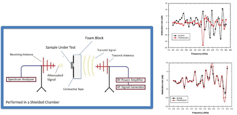
A Hot Filament Chemical Vapor Deposition (HF CVD) process was used to grow NCD films on 4 inch silicon, and fused silica (FS) at AKHAN Semiconductor. Prior to the NCD deposition, a nucleation pre-treatment was performed on the substrates through sonication using nanodiamond suspension in methanol for 20 mins. The wafers were subsequently rinsed in acetone, methanol, and isopropanol. A detailed process of the seeding and deposition processes can be found elsewhere [3]. For the HF CVD process, tungsten filaments with a diameter of 0.53 mm were heated to 2000 – 2400 °C by applying a bias voltage. The substrates were placed 20 mm below the filaments. The deposition of NCD was comprised of a three-step process involving carburization of the filaments, nucleation, and growth itself. For the rGO synthesis, a commercially obtained GO aqueous solution was spin-coated onto the NCD/Si and NCD/FS substrates. The samples were coated at a spin speed of 2000 RPM for 1 min and then baked at 100 °C for 1 min. To incorporate fluorine into the rGO layers, a plasma fluorination process was used, through an Oxford CCP- RIE plasma chamber with CHF3 and CF4 gas flows of 45 and 15 cm, respectively for 5 minutes. Chamber pressure was set to 30 mT, with an applied power of 50 W and a DC bias of 100 V. The morphology of the intrinsic silicon, GO, and the FGO structure was detailed by AFM and contact angle measurements. Both the measurements were conducted before and after the fluorination process. Next, A 532 nm laser was used for Raman characterization. Raman characterization was performed on the substrates at various stages of the fabrication processes, ahead of Fourier Transform Infrared Analysis. Lastly, EM testing was performed to measure relative electromagnetic loss in the 2 GHz to 8 GHz band at SportOn International (USA), Santa Clara in an isolation chamber to minimize the effect of background energy on the results. The test setup included a signal generator, two horn antennas, a spectrum analyzer, and a foam block to hold the sample under test.
Discussion
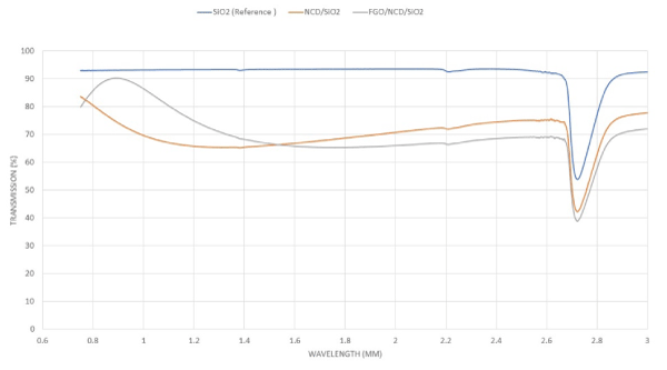
Contact angle derives a measure of hydrophobicity/hydrophilicity. The contact angle was measured to be 44 on GO films and after fluorination, the contact angle measured was 102 degrees. The FGO exhibits amphiphobicity, where the contact angle is above 90 degrees. The process of deriving FGO from GO can be extended for use in processing large area films. This method has been optimized for large area substrates. The fluorine atoms are covalently bonded to the GO films. The hydrophobicity also indicates that fluorine atoms have indeed been incorporated into the GO films as was seen in the previous reports, where the Raman transition from GO to FGO and associated contact angle changes are due to the presence of fluorine atoms. The thermal expansion coefficients of FGO and diamond are low with negligible lattice mismatch. This also makes the NCD/FGO multilayer a great candidate for operation at high temperatures (Figure 1).
As is seen in the resultant reflection losses, peak reflection losses of -12dB and -18dB were observed for the Si and FS samples, respectively. The observed reflectivity of the material is expressed as [4]
where
and where Zin is the input impedance of wave absorber and Z0 is that of free space
where
and where α is the attenuation constant, and β is the phase constant. The variation in reflection losses for the NCD vs. the FGO coated NCD are observed in Figure 2. Many factors could be contributing to the enhanced absorption of the FGO system as compared to the NCD system. In the case of FGO, is has been postulated that the effect of fluorination generates lattice defects and C-F clusters can act as polarization centers where the electromagnetic waves interact with the charge induced by fluorination which in turn produces polarization and attenuates electromagnetic wave leading to a good absorption Additional testing with different coating thickness and with different incident powers is needed for further study.
Conclusion
The current study is a demonstration of combining two extreme materials with extraordinary material properties, opening a new window for critical applications defense and space. We have successfully fluorinated reduced graphene oxide by spin coat dispersion and plasma fluorination, studying different surface morphologies with dramatic macroscopic changes to the measured contact angles, demonstrating selective tuning for hydrophobic/hydrophilic surfaces. Next, the FGO process was monolithically integrating with NCD films at wafer scales. The composite materials were studied for crystallographic quality, surface morphology, and optical transmissivity via Raman, AFM, and FTIR analysis, demonstrating high crystalline quality, sharp crystalline edges/stitching, and limited optical losses in the near to mid-infrared, respectively. Lastly, extreme EM absorption was obtained with FGO NCD composite on FS substrate as compared to the intrinsic Si, demonstrating through reflective losses the through electrical isolation capability of the FGO materials. The presented FGO diamond composite method, unlike most CVD graphene methods, is fully scalable and can be realized on the commercial level. With the material properties and large area capability now demonstrated, future studies will directly apply the materials to evolve.
Acknowledgment
This work was performed at AKHAN Semiconductor, and in part, in the Stanford Nanofabrication Facility, which is supported by the National Science Foundation as part of the National Nanotechnology Coordinated Infrastructure under award ECCS-1542152.
References
- Smith CJE, Higgs MS, Baldwin KR (1999) New metallic materials for the structure of aging aircraft. RTO MP-25.
- Coe SE, Sussmann RS (2000) Optical, thermal and mechanical properties of CVD diamond. Diam Relat Mater 9: 1726-1729.
- Lui H, Dandy DS (1995) Diamond CVD Techniques. William Andrew Publishing, USA, 14-45.
- Vinayasree S, Soloman MA, Sunny V, et al. (2013) Flexible microwave absorbers based on barium hexaferrite, carbon black, and nitrile rubber for 2-12 GHz applications. Compos Sci Technol 82: 69-75.
- Khan AH, Schirmann ES, Kovi KK (2021) Fluorinated graphene oxide, nanocrystalline diamond multilayer thin films for optical and electromagnetic limiting applications. Emergent Mater 4: 525-530.
Corresponding Author
Adam Khan, Founder and CEO, AKHAN Semiconductor, USA
Copyright
© 2021 Khan A. This is an open-access article distributed under the terms of the Creative Commons Attribution License, which permits unrestricted use, distribution, and reproduction in any medium, provided the original author and source are credited.