

Low-Cycle-Fatigue Failures of Solder Material in Electronics Packaging: Analytical Modeling Enables to Predict and Possibly Prevent Them-Review
Abstract
This review paper is based mostly on the author's recent publications and addresses the application of analytical ("mathematical") predictive modeling to understand the physics and mechanics of the behavior and performance of solder materials and solder joint interconnections employed in IC devices. The emphasis is on the design for reliability and, first of all, on the prediction of the thermal stresses and strains in solder joint interconnections in electronic products. While the majority of the numerous studies addressing solder materials are either experimental or based on finite-element-analyses (FEA), the approach considered in this review uses analytical predictive modeling techniques to predict stresses in solder interconnections and suggest methods for stress minimization. The developed models enable to come up with the most effective design-for-reliability methodologies to relieve the induced stresses and strains in solder joints of both levels of interconnections, and to predict, at the design stage, if inelastic strains in the solder material could be avoided. If not, these models are able to establish the sizes of the inelastic zones at the end portions of the soldered assemblies. It is concluded that all the three approaches of the applied science and engineering - experimental, computer-aided and analytical - are equally important from the standpoint of making a viable electron device into a reliable product, and that this review can explain how analytical modeling can be used in predicting and possibly preventing failures of solder joints in electronic products.
Review
Analytical ("mathematical") modeling, its significance, role, attributes and challenges
The overwhelming majority of studies dealing with the physical design and performance of "high-tech" materials and products are experimental. There are several good reasons for that: 1) Experiments could be carried out with full autonomy, i.e. without necessarily requiring theoretical support; 2) Unlike theory, testing can be used as a final proof of the viability and reliability of a product, and is therefore essential requirement, when it comes to making a viable device into a reliable product; 3) Experiments in the high-tech field, expensive as they might be, are considerably less costly than in other areas of engineering; 4) High-tech experimentations are much easier to design, organize, and conduct than in the macro-engineering world; 5) Materials, whose properties are, in effect, not completely known, are nevertheless often and successfully employed in high-tech products; 6) Every five years or so new generations of such products are developed, and there is often simply not enough time to establish all the properties and understand the behavior of materials in these products; lack of information about the material properties of electron devices is often an obstacle for carrying out modeling; 7) Many leading specialists in high-tech engineering (experimental physicists, materials scientists, chemists and chemical engineers, etc.) traditionally use experimental methods as their major research tool; it is not just a coincidence that eleven out of twelve Bell Labs Nobel laureates were experimentalists. Experimentation and proof-testing are viewed as supreme and ultimate judges of a product viability and reliability.
But experimental investigations, important as they are, 1) Require considerable time and significant expense; 2) Reflect the effect of the combined action of a variety of factors affecting the material, the phenomenon or the product of interest, and because of that might be insufficient to understand the underlying physics of the behavior of a material or a device of interest; 3) Experimental data cannot be simply extended to new materials, situations or designs, which are different from those already tested.
A simple, easy-to-use and physically meaningful model could be as practical and as trustworthy as the most thoroughly conducted experimentation. Such modeling, whether computer-aided or analytical, is or might be able to 1) Shed light on the role of each particular parameter that affects the behavior and performance of the material or the product of interest; 2) Predict the result of an experiment in less time and at considerably lower expense than the actual experiment; 3) Reveal superfluously reliable, "over-engineered", products that might be more costly than necessary and/or have excessive weight; 4) Discourage wasting time on useless experiments (the classical example are numerous attempts to build impossible heat engines that have been prevented by a study of the theoretical laws of thermodynamics); 5) Obtain valuable information about the phenomenon or the object, and provide an opportunity to decide, what and how should be tested or measured, and in what direction success might be expected; 6) Suggest new useful experiments (e.g., the theoretical analyses of thermal stresses in bi-material assemblies and in semiconductor thin films [1,2] triggered numerous experimental investigations aimed at the rational high-quality physical design of semiconductor crystal growth systems; 7) Interpret empirical results; 8) Bridge the gap between different experiments; 9) Extend the existing experience on new materials, components and structures; 10) Helpful when developing rational (optimal) designs (the idea of optimization of structures, materials, and costs has penetrated many areas of modern engineering, including electronics and photonics; no progress in this direction could be achieved, of course, without application of theoretical methods).
Analytical modeling [3-11] occupies a special place in the modeling effort. This is because it is able not only to come up with simple relationships that clearly indicate the role of various material and geometric characteristics of the design, but, more importantly, can often explain the underlying physics of phenomena and structures much better than the FEA or experimentation can. The limitations of a particular theoretical model could be often assessed based on a more general model: limitations of a linear approach could be determined on the basis of a more general non-linear model and the limitations of a deterministic approach can be assessed based on probabilistic modeling. Simplicity and clear physical meaning are crucial requirements for an effective analytical model. A good analytical model should be based on simple relationships that clearly indicate the role of the major factors affecting the phenomenon or the object of interest. While it is typically merely skills and training that are needed for the application of FEA, it takes a lot of imagination, intuition, knowledge, and significant effort to come up with a meaningful and practically useful analytical relationship.
Finite element analysis (FEA) has become the major modeling tool in electronics and photonics engineering. This should be attributed not only to the availability of powerful and flexible computer programs, which enable to obtain, within a reasonable time, a solution to almost any stress strain related problem, but also to the widespread illusion that FEA is the ultimate, indispensable and trustworthy tool for solving any stress analysis problem. The truth of the matter is that FEA and broad application of computers has by no means made analytical solutions unnecessary or even less important.
Simple analytical relationships have invaluable advantages, because of the clarity and compactness of the information. These advantages are especially significant when the parameter under investigation depends on several variables. As to the asymptotic analytical techniques, they can be successful in many cases, when there are difficulties in the application of computational methods, e.g., in problems containing singularities. Such problems are often encountered in high-tech materials engineering, because of the employment of assemblies comprised of dissimilar materials. But even when application of FEA encounters no difficulties, it is always advisable to investigate the problem analytically before carrying out FEA. Such a preliminary investigation helps to reduce computer time, develop the most feasible and effective FEA preprocessing model and, in many cases, avoid fundamental errors. It is noteworthy that FEA has been originally developed for structures with complicated geometry and/or with complicated boundary conditions (such as, e.g., avionics or some civil engineering structures), when it might be difficult to apply analytical approaches. As a consequence, FEA has been especially widely used in those areas of engineering, in which structures of complex configuration are typical (aerospace, maritime and offshore structures, some civil engineering structures, etc.). In contrast, electronic and photonic structures are usually characterized by simple geometries and can be easily idealized as beams, flexible rods, rectangular or circular plates, composite structures of relatively simple geometry, etc. There is an obvious incentive therefore for a broad application of analytical modeling in electronics and photonics structural analysis. Additional incentive is due to the fact that adjacent structural elements in electronics and photonics engineering have dimensions that differ by orders of magnitude. Examples are multilayer thin film structures fabricated on thick substrates or adhesively bonded assemblies, in which the bonding layer is significantly thinner than the bonded components. Since the mesh elements in a FEA model must be compatible, FEA of such structures often becomes a problem of itself, especially in regions of high stress concentration. Such a problem does not occur, however, with an analytical approach. Another consideration in favor of analytical modeling is associated with an illusion of simplicity in applying FEA procedures. Many users of FEA programs sincerely believe that the FEA "black box" they deal with will always provide the right answer. It is well known, however, that although it might be easy to obtain a FEA solution, it might be quite difficult to obtain the right solution. And how would one know that it is indeed the right solution, if there is nothing to compare it with?
Clearly, if the FEA data are in good agreement with the results of an analytical modeling, then there is a reason to believe that the obtained solution is accurate enough and is trustworthy. FEA data and analytical solutions are typically based on different assumptions: FEA is a numerical continuum mechanics tool, while the available close-form analytical solutions, including those addressed in this review, use mostly approximate structural analysis and strength-of-materials methods, which are usually different in different problems. Therefore, good agreement of the FEA and analytical data is usually an indication that the obtained solution reflects the actual state of stress.
Method of interfacial compliance (MIC)
Method of interfacial compliance (MIC) [1,2,12-18] suggested back in 1986 [1,2,19] is an extension of the 1925 Timoshenko analysis [11] of bi-metal thermostats. Timoshenko's theory was developed for long-and-narrow assemblies, and only the normal stresses acting in the cross-sections of the bonded strips were determined. As to the interfacial stresses, Timoshenko indicated in his paper that they could not be found in an elementary fashion, and that theory-of-elasticity had to be employed to address them. The obtained later on theory-of-elasticity solutions were, however, so cumbersome that one had to resort to a computer to obtain numerical data from these solutions. Then, why not use FEA, which is applied directly to the structure of interest?
Unlike Timoshenko's theory, MIC considers assemblies of finite size and with an emphasis on their bow (warpage) and the interfacial shearing and peeling stresses. The MIC enables to obtain an accurate enough engineering method for the evaluation of the assembly bow and the distributed interfacial stresses. MIC uses simple and approximate structural analysis (strength-of-materials) techniques, rather than general and rigorous theory-of-elasticity concepts. The MIC enables to separate the "internal" (geometrical and material properties related) factors from the "external" (change-in-temperature related) ones. The application of the MIC results in simple closed-form solutions that clearly indicate the role of different characteristics of the assembly and the loading conditions.
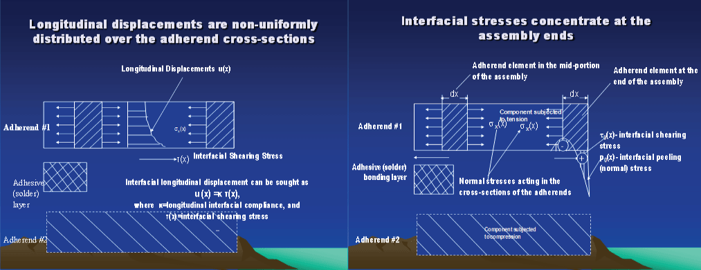
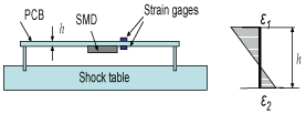
The MIC considers that the longitudinal interfacial displacements of the assembly components are non-uniformly distributed over the components' cross-sections (Figure 1, left sketch) and that the interfacial points of the given cross-section of the bonded component have larger longitudinal displacements than the inner points of this cross-section. It is also postulated that the deviations of the given cross-section from planarity can be sought as the product of the (longitudinal coordinate independent) interfacial compliance of the given assembly component and the sought interfacial shearing stress at the given cross-section. Right sketch in Figure 1 shows that the interfacial shearing stresses concentrate at the assembly ends, and the MIC confirms this physically obvious circumstance.
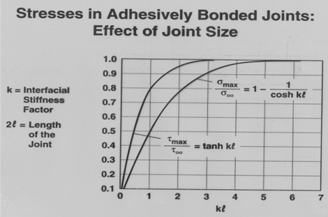
The MIC uses the notion of the parameter k of the interfacial shearing stress and predicts that the maximum values of the interfacial thermal stresses increase with an increase in the assembly size for short assemblies with compliant bonds, but remain unchanged for large enough assemblies with stiff interfaces, as long as the product kl of the parameter k and half the assembly length l exceeds the kl ≈ 2.5 level (Figure 2). A simple, easy-to-use and physically meaningful formula was obtained for the interfacial shearing stress in the case of the plane stress approximation. In this formula, is the force (per unit assembly width) acting in the cross-sections of the mid-portion of a long assembly (kl ≥ 2.5), ∆α is the CTE difference of the bonded materials, ∆t is the change in temperature, λ = λ1 + λ2 is the total axial compliance of the assembly, and are the axial compliances of the assembly components, and are the component thicknesses, E1 and E2 are Young's moduli of the materials, v1 and v2 are their Poisson's ratios, is the parameter of the interfacial shearing stress, κ = κ0 + κ1 + κ2 is the total interfacial compliance of the assembly, is the interfacial compliance of the bonding layer, and are the interfacial compliances of the assembly components, , and are shear moduli of the materials of the adhesive and the two adherends, and l is half the assembly length. The origin of the longitudinal coordinate x is at the mid-cross-section of the assembly.
The formula for the parameter k of the interfacial shearing stress indicates that this parameter and, hence, the interfacial shearing stress itself, increase with an increase in the axial (longitudinal) compliance of the assembly and decreases with an increase in its interfacial compliance. This simple relationship reflects the well-known fact that the best, from the standpoint of the induced stresses, bonded assembly is characterized by stiff adherends and compliant adhesives.
The above formula for the interfacial shearing stress can be simplified as in the case of long assemblies with stiff interfaces, and as in the case of short assemblies with compliant interfaces. The first formula indicates that the elevated shearing stress in a long assembly concentrates at its ends and does not change with an increase in the assembly size. The second formula indicates that, in the case of a short assembly, the interfacial shearing stress increases linearly with an increase of the distance from the mid-cross-section of the assembly. The maximum stress in a long assembly takes place at the assembly ends and is . For assemblies characterized by the kl values exceeding 2.5 this formula yields: , so that the maximum stress becomes assembly size independent (Figure 2).
It has been shown analytically and confirmed by FEA that the interfacial shearing stress can be evaluated without considering its coupling with the peeling stress, and that the latter can be evaluated from the calculated shearing stress. It has been shown also that the interfacial peeling stress is proportional to the longitudinal gradient of the shearing stress.
The concept of the interfacial compliance was extended to thin films fabricated on thick substrates; to bonded assemblies with identical adherends, including inhomogeneous bonds; to tri-material assemblies and to other cases, when there was a need to evaluate the thermally induced stresses in bonded assemblies comprised of dissimilar materials. As a rule, excellent agreement between the analytical and FEA predictions has been observed.
Soldered assemblies with identical adherends
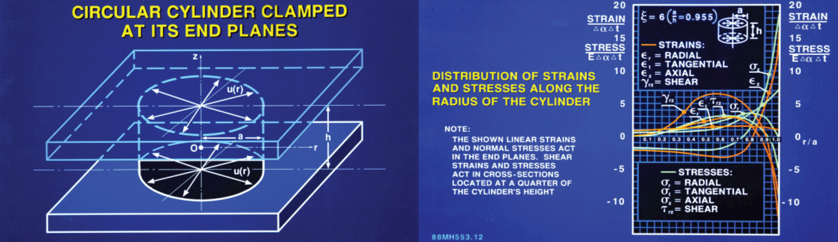
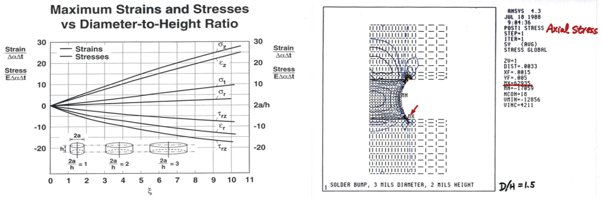
There is an obvious incentive to employ thermally matched materials in an electronic assembly for lower thermal stresses in solder joints. Such an assembly was indeed considered and tested in the Bell Labs Si-on-Si flip-chip technology [20,21] (Figure 3, Figure 4, Figure 5 and Figure 6). It has been assumed that a short circular cylinder adequately represents a solder bump, and analytical modeling was used to predict the stresses and strains in such a cylinder [22]. It has been shown particularly that joints characterized by elevated stand-off heights exhibit lower stresses and strains than "pancake-like" joints (Figure 5 left). The analytical results were confirmed by FEA data (Figure 5 right). The expected meniscus in the joint experiencing low temperature conditions can be seen in Figure 5 right. Clearly, the highest stresses take place at the extreme corners of the joint.
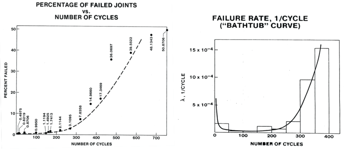
FOAT tests were carried out and their results are shown in Figure 6 left. Such tests are usually conducted until half of the population fails. The experimental bathtub curve is shown in Figure 6 on the right. It is important that about half of the solder material lifetime is under the wear-out condition. This result indicates that the wear out portion of the bathtub curve for solders should be considered in the design-for-reliability effort of solder joints. At that time tin-lead solders were considered and tested. The calculated probabilities of failure are shown in Table 1. Failures were detected by electrical measurements.
Inelastic strains in solder material
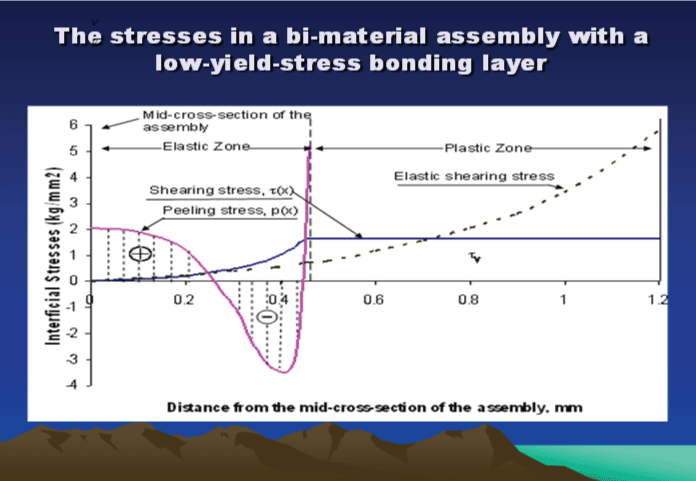
As far as the long-term reliability of a soldered assembly as a whole is concerned, it makes a difference, if just one or more peripheral solder joints experience inelastic strains: the low cycle fatigue lifetime of the solder system is inversely proportional to the number of joints that are simultaneously subjected to inelastic strains. A simple and physically meaningful formula is obtained [23,24] for the prediction, at the design stage, of the number of such joints, if any, for the given effective thermal expansion (contraction) mismatch of the package and PCB; materials and geometrical characteristics of the assembly and its size; and, of course, the level of the yield stress of the solder material. When half the length le of the elastic portion of the assembly is large and/or the parameter k of the interfacial shearing stress is significant (kl ≥ 2.5), which is typically the case in actual SMD assemblies, the following simple formula for the length lY of the inelastic zone has been obtained: . Here is the maximum interfacial shearing stress calculated under an assumption that no inelastic strains occur and τY is the yield stress in shear of the solder material. This formula can be used, first of all, to determine if, by the proper selection of the above characteristics the inelastic strains in the solder could be avoided and, if not, how many peripheral joints will most likely experience inelastic strains. The distribution of the thermal interfacial stresses is shown in Figure 7 for a bi-material soldered assembly with a low-yield-strain of the bonding layer.
The interfacial peeling stress is self-equilibrated within the elastic mid-portion of the assembly and, because the peeling stress is proportional to the longitudinal gradient of the shearing stress, becomes zero at the peripheral plastic zones, where the shearing stress is constant.
Elevated stand-off heights can relieve stress in solder joints
Physically meaningful and easy-to-use analytical (mathematical) stress model is developed for a short beam with clamped and offset ends [25]. The analysis is limited to elastic deformations. While the classical Timoshenko short-beam theory seeks the beam's, deflections caused by the combined bending and shear deformations for the given loading, an inverse static problem is considered here: the lateral force is sought for the given ends offset. In short beams this force is larger than in long beams, since, in order to achieve the given displacement (offset), the applied force has to overcome both bending and shear resistance of the beam. It is envisioned that short beams could adequately mimic the state of stress in solder joint interconnections, including ball-grid-array (BGA) systems, with large, compared to conventional joints, stand-off heights.
When the package/printed-circuit-board (PCB) assembly is subjected to the change in temperature, the thermal expansion (contraction) mismatch of the package and the PCB results in an easily predictable relative displacement (offset) of the ends of the solder joint. This offset can be determined from the known external thermal mismatch strain (determined as the product of the difference in the coefficients of thermal expansion of the assembly components and the change in temperature) and the position of the joint with respect to the mid-cross-section of the assembly. The maximum normal and shearing stresses could be viewed as suitable criteria of the beam's (joint's) material long-term reliability. It is shown that these stresses can be brought down by employing beam-like joints, i.e., joints with an increased stand-off height compared to conventional joints, and, hence, with an increased longitudinal interfacial compliance. It is imperative, of course, that, if such joints are employed, there is still enough interfacial real estate, so that the BGA bonding strength is not compromised. On the other hand, owing to the lower stress level, reliability assurance might be much less of a challenge than in the case of conventional joint configuration. By employing beam-like solder joints one can even manage to avoid inelastic deformations of the joints, thereby increasing dramatically their fatigue lifetime.
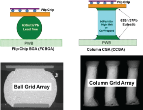
The numerical example was carried out in [25] with the following input data: the CTE of the package and the PCB are 12 × 10-61/℃ and 18 × 10-61/℃, respectively, the change in temperature from the reflow soldering (fabrication) temperature to the room temperature is 275 ℃, and the distance from the package mid-cross-section to the location of the given solder joint of the BGA system is 12 mm. The predicted thermally induced end offset of the solder joint is ∆ = (18 × 10-6 – 12 × 10-6) × 275 × 12 ≈ 0.02 mm. With the Young's modulus and the Poisson's ratio of the solder material of E = 30 GPa = 3060 kg/mm2 and v = 0.30, the height of the solder joint of h = 0.8 mm, and half the solder joint thickness of l = 0.2 mm, the calculated data yield: τmax = 37.1 kg/mm2 and σ = 148.3 kg/mm2. If the stand-off height is increased to h = 1.6 mm, then the predicted stresses are τmax = 3.7 kg/mm2 and σ = 29.7 kg/mm2. The change is indeed significant, and if a BGA is replaced by a column-grid-array (CGA) (Figure 8) [26], there is a good chance that inelastic strains in the solder material could be avoided. There is even a possibility that, because of the relief in the interfacial stresses and in the warpage of the assembly, its propensity to the recently observed head-in-pillow (HiP) defects will also be diminished.
Application of inhomogeneous bonds
Another, perhaps, the most effective, way to bring down the interfacial stresses in soldered assemblies is to design and employ inhomogeneous solder joint interconnection systems [27-37]. This could be done by using low modulus and/or, if possible and economically feasible, also low fabrication temperature materials at the peripheral portions of the solder system [27-32] and/or, strange as it may sound, by increasing the interfacial stiffness of its mid-portion [33]. This is, because of the stiffer mid-portions, the peripheral interfacial displacements will be decreased, and so will the interfacial stresses be. It is imperative, however, that such a possible relief is predicted by using the suggested design-for-reliability methodologies and preferably confirmed by FEA data. If such a prediction is not done, an intuitive application of an in-homogeneous bond could very well result in more harm than good.
The expected stress relief could be even optimized [34] by designing the solder system in such a way that the predicted shearing stress at the boundary between the mid-portion and the peripheral portions of the assembly is made equal to the shearing stresses at the assembly ends. Calculations indicate that these two stresses could be significantly lower than the stresses at the ends of an assembly with a homogeneous bond, even when the interfacial compliance of such a bond is as high as the compliance of the low-modulus peripheral portions of an in-homogeneous bond. This statement is in agreement with the message of the ref. [33]. Various possible ways to minimize stresses in solder joint systems were summarized and explained in Ref. [35].
An important "theoretical" question that arises in connection with modeling thermal stresses in solder joint interconnection is whether thermal stresses in real life, certainly and always "inhomogeneous" (because of the gaps/spaces between the joints) solder joint interconnections be predicted, with sufficient accuracy, by using relatively simpler models developed for homogeneous adhesively bonded or soldered assemblies. It has been shown [36] that such a substitution is acceptable, if the gaps between the supports (BGA balls or CGA columns) are small, and the product kl of the parameter k of the interfacial shearing stress and half the assembly length l is significant, such a simplification is acceptable. Practically, the following "rule of thumb" can be used: if the ratio p/2l of the pitch/space p (distance between the joint centers) to the joint widths 2l is below 5, and the parameter kl is above 2.5, which is indeed the case in actual BGA and CGA systems, then the predictions based on the simplification assuming homogeneous/continuous bonds is accurate enough.
The induced stresses in mirror-like package designs were addressed in [37].
Flip-chip designs
Flip-chip designs, from the standpoint of the most suitable encapsulants and the induced stresses, were addressed first back in 1990 [38], including the incentive for bringing in underfills. The bonding layer in today's flip-chip assembly designs with various underfills is characterized by a relatively high effective Young's modulus of its composite material, which is comprised of high-modulus solder and relatively low-modulus epoxy encapsulant/undrfill. The objective of the analysis carried out in Ref. [39] was to determine if a bi-material model [2,11,19] could be used for the analysis of stresses in the solder joints of such a design, or a more complicated tri-material model [14] should be employed. While in a tri-material model all the three materials -the chip, the substrate and the bonding layer- are "equal partners", in a bi-material model a significant simplification is made, assuming that the bonding layer is much thinner than the bonded components, the chip and the substrate, and that its effective Young's modulus is significantly lower than the moduli of the chip and the substrate materials. In the carried out numerical example [39] based on the application of the tri-material model, the highest shearing stress occurs at the chip-bond interface and is significantly, by the factor of about 2.45, higher than the stress at the substrate-bond interface, but even the latter stress is about twice as high as the maximum shearing stress predicted on the basis of the bi-material model. As to the normal stresses acting in the cross-sections of the assembly components, the tri-material model predicts that the highest stresses occur in the chip, the lowest - in the substrate, and that the stresses in the bond are rather high, about 59% of the stresses in the chip. The bi-material model, however, simply assumes that the normal stresses in the bond are zero. The normal stresses in the chip predicted on the basis of the bi-material model are only about 78% of the stress predicted by the tri-material model. The normal stresses in the substrate evaluated on the basis of the bi-material model are almost twice as high as the tri-material model predicts, but these stresses are low anyway: it is the state of stress in the chip and in the bonding layer, and the interfacial stress at the chip-bond interface that should be of concern to the device designer. It is concluded that while a simple bi-material model can be successfully used for adhesively bonded assemblies, a tri-material model should be employed for flip-chip assemblies, especially when high-modulus solders are used. Ways to evaluate and to relieve stresses in flip-chip solder joints were addressed and discussed in [40,41], considering quite complicated configurations of the today's most typical flip-chip designs.
Accelerated testing of solder joint interconnections: Board level dynamic tests
Board level drop test was considered [42,43] with an objective to develop a physically meaningful analytical predictive model for the evaluation of the expected impact-induced dynamic stresses in the solder material (Figure 9).
Ball-grid-array (BGA) and column-grid-array (CGA) designs were addressed. Intuitively it is felt that while the application of the CGA technology to relieve thermal stresses in the solder material might be quite effective (owing to the greater interfacial compliance of the CGA in comparison with the BGA), the situation might be different when the PCB/package experiences dynamic loading. This is because the mass of the CGA joints exceeds considerably that of the BGA interconnections and the corresponding inertia forces might be considerably larger in the case of a CGA design. The numerical example carried out for rather arbitrary, but realistic, input data has indicated that the dynamic stresses in the solder material of the CGA design are even higher than the dynamic stresses in the BGA interconnections. This means particularly that the physically meaningful drop height in board-level tests should be thoroughly selected and that this height should be different, when BGA and CGA designs are considered. The predicted dynamic shearing stress is by about 6.7% higher, and the predicted peeling stress is by about 5.5% higher, when the CGA technology is used, as compared to the BGA design. The analytical stress models can be of help when designing and building experimental vehicles for thermal and dynamic testing of BGA and CGA interconnections.
Accelerated testing of solder joint interconnections: Solder material characterization
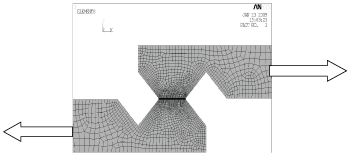
A simple analytical model has been developed to explain a paradoxical situation that has been detected on the basis of the finite element analysis (FEA) by Jorma Kivilahti and Tommi Reinikainen [44]: deep enough transverse grooves in the adherends ("pins") resulted in an appreciable reduction in, and to the more uniform distribution of, the interfacial shearing and peeling stresses (Figure 10). This phenomenon, important from the standpoint of testing solder materials, was explained based on analytical modeling by Suhir and Reinikainen [45,46].
The model indicates that the "observed" phenomenon is due primarily to the increase in the interfacial compliance of the bonding structure: the grooves "convert" the adherend ("pin") portions located between the inner portions of the grooves and the bonding (adhesive, solder) layer into parts of the bonding structure, thereby increasing the compliance of this structure with respect to the shearing load. This positive effect overwhelms, as far as the magnitude and the distribution of the interfacial stresses are concerned, the negative effect of the increased axial compliance of the loaded portions of the adherends ("pins"), because of the grooves.
The analytical predictions agree well with the FEA data, despite the FEA overestimation of the increase in the interfacial stresses in the proximity of the joint edges (as is known, FEA method, which is based on one of the numerical methos of the elasticity theory, leads to singular stresses at the edges of assemblies comprised of dissimilar materials).
The obtained information explains the physics of the phenomenon in question, and the developed analytical models can be used in the analysis and physical design of soldered lap shear joints. It is concluded also that analytical modeling is able not only to come up with relationship that clearly indicate "what affects what and what is responsible for what", but, more importantly, can explain the physics of phenomena that neither the FEA modeling ("simulation"), nor even actual experimentation is able to. It is recommended that such tests are considered to obtain the mechanical properties of the solder materials for further analytical or FEA modeling.
Accelerated testing of solder joint interconnections: Failure-oriented accelerated testing (FOAT) and highly-accelerated-life-testing (HALT)
A highly focused and highly cost effective FOAT [47-50], which is the experimental foundation and the "heart" of the recently suggested PDfR concept [51-64] should be conducted in addition to and, in some cases, even instead of HALT, especially for highly vulnerable materials, like solders, and for new products, whose operational reliability is unclear, for which no experience is accumulated and no best practices nor HALT methodologies are not yet developed. Predictions, based on the FOAT and subsequent probabilistic predictive modeling, might not be perfect, especially at the beginning, but it is still better to pursue this effort rather than to turn a blind eye on the fact that there is always a non-zero probability of the product's failure. Understanding the underlying reliability physics for the performance of the material and product of importance is critical. If one sets out to understand the physics of failure in an attempt to create a practically failure-free product (in accordance with the "principle of practical confidence"), conducting a FOAT type of an experiment is imperative.
FOAT's objective is to confirm the usage of a particular predictive model, to confirm (say, after HALT is conducted) the physics of the material failure, and to establish the numerical characteristics (activation energy, time constant, sensitivity factors, etc.) of the particular FOAT model of interest. FOAT could be viewed as an extension of HALT. While HALT is a "black box", i.e., a methodology which can be perceived in terms of its inputs and outputs without a clear knowledge of the underlying physics and the likelihood of failure. FOAT, on the other hand, is a "transparent box". The major assumption is, of course, that the FOAT model should be valid in both accelerated test and in actual operation conditions. HALT does not measure (does not quantify) reliability. FOAT does. HALT can be used therefore for "rough tuning" of material's/product's reliability, and FOAT could be employed when "fine tuning" is needed, i.e., when there is a need to quantify, assure and even specify the operational reliability of a material or a product.
HALT tries to "kill many unknown birds with one (also not very well known) stone". HALT has demonstrated, however, over the years its ability to improve robustness through a "test-fail-fix" process, in which the applied stresses (stimuli) are somewhat above the specified operating limits. This "somewhat above" is based, however, on an intuition, rather than on a calculation. There is a general perception that HALT might be able to quickly precipitate and identify failures of different origins. FOAT and HALT could be carried out separately or might be partially combined in a particular AT effort. Since the principle of superposition does not work in reliability engineering, both HALT and FOAT use, when appropriate, combined stressing under various stimuli (stressors). New products present natural reliability concerns, as well as significant challenges at all the stages of their design, manufacture and use.
An appropriate combination of HALT and FOAT efforts could be especially useful for ruggedizing and quantifying reliability of such products. It is always necessary to correctly identify the expected failure modes and mechanisms, and to establish the appropriate stress limits of HALTs and FOATs with an objective to prevent "shifts" in the dominant failure mechanisms. There are many ways of how this could be done (see, e.g., next section, suggesting mechanical pre-stressing of FOAT specimens subjected to temperature cycling). The FOAT based approach could be viewed as a quantified and reliability physics, oriented HALT. The FOAT approach should be geared to a particular technology and application, with consideration of the most likely stressors.
Accelerated testing of solder joint interconnections: Incentive for mechanical pre-stressing of accelerated test specimens
Accelerated testing of soldered assemblies, such as, e.g., temperature cycling, is usually conducted in a wider range of temperatures than is expected to take place in actual operation conditions. Since the mechanical and electrical properties of electronic materials are temperature sensitive, such testing might generate deviations of the material properties from the properties that they possess in actual operations conditions, and the results of such accelerated testing might be misleading: they might trigger mechanisms and modes of failure that will never occur in the field conditions. In such a situation mechanical pre-stressing of the accelerated test specimens [55] might be a promising way to go. FOAT specimens are particularly vulnerable, since the temperature range in these tests should be broad enough to eventually lead to failures, and if a shift in the modes and mechanisms of failures takes place during significant temperature excursions, the physics of such failures might be quite different than in actual operation conditions. An appropriate mechanical pre-stressing can be an effective means for narrowing the range of temperature excursions during accelerated testing and, owing to that, -for obtaining consistent and trustworthy test data. If such a pre-stressing is considered and implemented, the ability to predict/model the thermomechanical stresses in the test specimen is certainly a must.
Accelerated testing of solder joint interconnections: Incentive for using a low-temperature/random-vibrations bias
Although there exist promising ways to avoid inelastic strains in solder joints of the second level interconnections in IC package designs, it still appears more typical than not that the peripheral joints of a package/PCB assembly experience inelastic strains. This takes place at low temperature conditions, when the deviation from the high fabrication temperature is the largest and the induced thermal stresses are the highest. On the other hand, it is well known that it is the combination of low temperatures and repetitive dynamic loading that accelerate dramatically the propagation of fatigue cracks, whether elastic or inelastic. Accordingly, a modification of the recently suggested Boltzmann-Arrhenius-Zhurkov (BAZ) model [50-62] is developed for the evaluation of the remaining useful lifetime (RUL) of the second level solder joint interconnections whose peripheral joints experience inelastic strains. The experimental basis of the approach is the highly focused and highly cost-effective failure-oriented-accelerated-testing (FOAT). The FOAT specimens have been subjected in our methodology (which is "reduced to practice") to the combined action of low temperatures (not to elevated temperatures, as in the classical Arrhenius model) and random vibrations with the given input energy spectrum.
The suggested methodology is viewed as a possible, promising, effective and attractive alternative to temperature cycling tests. As long as inelastic deformations are inevitable, it is assumed that it is these deformations that determine the fatigue lifetime of the solder material, and the state of stress in the elastic mid-portion of the assembly does not have to be accounted for. The roles of the size and stiffness of this mid-portion have to be considered, however, when determining the very existence, the inelastic zones at the peripheral portions of the design and establishing their size. The general concept is illustrated by a numerical example. Although this example is carried out for a ball-grid-array (BGA) design, it is applicable to highly popular column-grid-array (CGA) and quad-flat-no-lead (QFN) designs as well. It is noteworthy that it is much easier to avoid inelastic strains in CGA and QFN structures than in the addressed DGA design. The random vibrations are considered in the developed methodology as a white noise of the given ratio of the acceleration amplitudes squared to the vibration frequency. The suggested model is confirmed by accelerated testing. Testing was carried out for two PCBs, with surface-mounted packages on them, at the same level (with the mean value of 50 g) of three-dimensional random vibrations. One board was subjected, concurrently with random vibrations, to the low temperature of -20 ℃ = 253 ºK and another one - to -100 ℃ = 173 ºK. It has been predicted, by preliminary calculations using the developed model that the solder joints at the -20 ℃ will still perform within the elastic range, while the solder joints at -100 ℃ will experienced static inelastic strains. No wonder that no failures were detected in the solder joints of the board tested at -20 ℃ while the joints of the board tested at -100 ℃ failed after several hours of testing. Some results of such an accelerated testing are addressed, described and commented on. Here is how FOAT could be implemented in the problem in question.
Let us assume that the failure rate of the solder material, which characterizes the rate of propensity of the material or the device to failure, could be monitored determined by the level of the measured electrical resistance: λ = γRR.
Using the BAZ model [51-62] and considering the combined action of low temperature T (that supposedly leads to elevated thermal stresses in the solder material) and external random vibrations characterized by their spectrum S one can seek the probability of the material non-failure after FOAT for the time t in the form:
where the values reflect the sensitivities of the material to the corresponding stimuli (stressors), and R is the continuously measured/monitored electrical resistance for the peripheral joints. Although only two stimuli (stressors) were selected in this model- low temperature and random vibrations-, the model can be easily made multi-parametric, i.e., generalized for as many stimuli as necessary. The units for the sensitivity parameter γR are obviously Ω-1hr-1, if the measured electrical resistance of the peripheral solder joints is measured in ohms, and the elapsed time t is measured in hours. The unites of the sensitivity parameter γS are eV m-2sec-3, if the stress-free activation energy U0 is measured in eV and the power spectral density (PSD) amplitudes are measured in (m/sec2)2/Hz = m2sec3. The physical meaning of the above distribution could be seen from the formulas
where H(P) = -Pln P is the entropy of the probability P of non-failure. Thus, the change in the probability of non-failure always increases with an increase in the entropy (uncertainty) of the distribution and decreases with an increase in the monitored (measured) electrical resistance and the elapsed time. As to the sensitivity factor γS, it can be found as the ratio of the (negative) derivative of the probability of non-failure with respect to the level of the vibration excitation (power spectrum) to the ratio of the entropy of the probability of non-failure to the level of the thermal energy kT. It should be emphasized that the temperature T in the above formulas is, unlike in the Boltzmann's statistics or in the Arrhenius formula, a parameter, not an argument. It is the threshold of the low temperature, below which the inelastic strains in the peripheral solder joints occur. This temperature/threshold should be determined and established based on the procedures addressed in the above "Inelastic strains in solder material" section. The expression for the probability of non-failure contains three empirical parameters: the stress-free activation energy U0 and two sensitivity factors, γR and γS. Here is how these parameters can be obtained from the conducted highly focused and highly cost effective FOAT data.
At the first step one should run the FOAT for two different temperatures T1 and T2 keeping their levels unchanged during the experiment. Unlike in the original Arrhenius or in Zhurkov's experiments, these levels should be established and kept low enough, so that inelastic strains in the peripheral solder joints of the package/PCB assembly could occur. These temperatures could/should be obtained from the preliminary thermal stress analysis described above. Recording the percentages (values) P1 and P2 of non-failed samples (or values Q1 = 1 - P1 and Q1 = 1 - P2 of the failed samples) and assuming a certain criterion of failure (say, when the level of the measured electrical resistance, because of the "opens" in the failed joints, exceeds a certain level R1 one could obtain the following two relationships:
Since the numerators U0 - γSS (effective activation energies) in these relationships are kept the same during the FOAT, the following equation must be fulfilled for the sought sensitivity factor γR of the electrical resistance:
Here t1 and t2 are times, at which the failures defined as the moments of time when the level R* of the continuously measured electrical resistance, were observed. The above equation has the following solution:
It is expected that more than two series of FOAT tests and at more than two temperature levels should be conducted, so that the sensitivity parameter γR could be established with a high enough degree of accuracy and certainty.
At the second step, FOAT tests at two spectra levels S1 and S2 should be conducted for the same temperature T. This leads to the relationship:
Note, that the γS value is independent, in this approach, of the resistance R* threshold and the sensitivity factor γR. Finally, the stress-free activation energy can be computed, for the determined factors γR and γS as for any consistent vibration spectrum level, temperature threshold and time values. After the sensitivity factors and the loading (stressor) free activation energy are determined for the tested combinations of the input data, the above formula could be used, but should be checked (validated), of course, for other physically meaningful combinations of the FOAT parameters. The fatigue lifetime can be found for the induced temperature below the temperature, at which the inelastic strains occur, from the basic formula for the probability of non-failure as follows:
This formula makes physical sense. Indeed, the RUL increases with an increase in the probability P of non-failure, and with an increase in the level of the effective activation energy U = U0 - γSS. The RUL decreases with an increase in the acceptable level R* of the electrical resistance of the damaged joints, with an increase in the sensitivity factor γR and the level kT of the thermal energy. This level is higher for lower thermal energies.
The numerical example that follows is carried out with the following input data Table 2.
And here are the computed data:
Axial compliances of the assembly components:
Flexural rigidities of the assembly components:
Total axial compliance of the assembly:
Interfacial compliances:
Parameter of the interfacial shearing stress
The product kl = 0.9890x15.0 = 14.8350 is significant, and therefore the maximum interfacial shearing stress can be evaluated assuming infinitely large assembly.
For the board tested at -20 ℃ this stress is
and is somewhat below the yield stress of the solder material, so that no inelastic strains are likely to occur. For the board tested at -100 ℃ this stress is
and the lengths of the inelastic zones in this case are
The temperature boundary between the elastic and inelastic states of stress is characterized by the temperature change of
and, with the soldering temperature of -158 ℃, is -24.6 ℃.
Here is a hypothetical example of how the parameters of the BAZ equation can be determined, when testing is conducted until failure. Note that has not been the case for the two PCBs whose testing is described in the Test Procedure and Data below, since only the solder joints in the PCB tested at -100 ℃ have failed, while the joints in the board tested at -20 ℃ have not exhibit any failure after many hours of testing. Let, e.g., the FOAT is carried out until the resistance threshold is reached. Half of the specimen population failed at the first stage of testing at the temperature of T1 = -30 ℃ = 243 °K after t1 = 200 hrs of testing. When testing was conducted at the temperature of T2 = -10 ℃ = 263 °K, half of the specimen population failed after t2 = 300 hrs of testing. The level of the vibration power spectrum density was kept the same in both sets of the tests and did not affect therefore the factor γR. Then the equation for the sensitivity parameter γR yields:
The thermal energy is kT1 = 8.6176x10-5 × 243° = 2.941 × 10⁻² eV, when testing is carried out at the temperature T1 = -30 ℃ = 243 °K and is kT2 = 8.6176 × 10-5x263° = 2.2664 × 10⁻² eV, when testing is carried out at the temperature T2 = -10 ℃ = 263 °K. Let the testing at the second stage of testing be carried out until 99% of the tested specimens failed, so that P = 0.01, and that this took place after t1 = 500 hrs of testing at the temperature of T1 = -30 ℃ = 243 °K and at the vibration level of S1 = 2 × 106 mm2sec-3 and after t1 = 650 hrs of testing at the temperature of T2 = -10 ℃ = 263 °K and at the vibration level of S2 = 106 mm2sec-3. The effective activation energy is
when testing was carried out at the temperature T1 = -30 ℃ = 243 °K, and is
when testing was performed at the temperature T2 = -10 ℃ = 263 °K. Clearly, since the thermal strain and/or the region occupied by the inelastic stresses in the solder material are higher at the lower temperature condition, the remaining effective activation energy is lower at this temperature.
From the last two equations, considering that the zero-stress activation energy should be loading independent, we have the following formula for the vibration sensitivity factor:
Then the stress-free activation energy can be computed as
or as
The remaining useful life can be computed for any probability of non-failure, low temperature and vibration spectral density as
If, e.g., P = 0.9, T = -20 ℃ = 253 °K, and S = 103 mm2sec-3, then the predicted RUL of the solder material is
The actual testing has been carried out at the Reliant Labs, Inc., 925 Thompson Place, Sunnyvale, CA. Two PCB boards, serial numbers QFN-P-07 and QFN-P-08, provided by the customer, were tested. Qualmark OVS 2.5LF HALT/HASS Chamber (model # 2.5LF) was used to accommodate the test specimens (one at a time). Omega thermocouples were used to measure temperature, and Dytran accelerometer control was used to measure the applied accelerations. All test equipment that requires periodic calibration was in current calibration at time of test.
The test results could be summarized as follows. Board #1 was tested at the temperature of -20 ℃ and the (identical) board #2 at the temperature of -100 ℃. In both cases the established level of the random 3D vibrations was 50 g. The reason why these temperatures were chosen, is that, according to the above calculations, the -20 ℃ temperatures were not expected to lead to inelastic static strains, while the -100 ℃ temperature was supposed to result in appreciable plastic deformations and, hence, in a considerably shorter fatigue life of the solder material. Electrical resistance was continuously measured in four corner packages of each board. Prior to testing all the joints showed resistance of about 0.15 µΩ. For the board #1 (tested at -20 ℃) this level of resistance has not changed after five hours of testing. For the board #2 (tested at -100 ℃) opens in two packages were detected after about 1.5 hours of testing, and an increase in the resistance to about 0.9 Ω was detected for the remaining two corner packages after about 3.5 hours of testing. The total time of testing of the board #2 was about 4.0 hours.
Hence, the test results have confirmed the general concept that low temperatures in combination with random vibrations might be an attractive accelerated test vehicle for electronic materials and packages, and that there is a significant difference in the fatigue lifetime (remaining useful life) for the solder material that remains within the elastic region (when subjected to moderately low temperatures) and the material that is stressed above this region at significant low temperatures. The tests were not continued beyond the above times, since no substantial new information was expected if they would be. It should be emphasized, however, that the FOAT should be always conducted, if there is an intent to quantify the RUL. For materials that failed within the elastic region the probabilistic Palmgren-Miner "rule of the linear accumulation of damages" [65] can be used to predict the RUL.
Conclusion
All the three approaches of the applied science and engineering-experimental, computer-aided and analytical - are equally important from the standpoint of making a viable electron device into a reliable product. The review can explain how predictive modeling approach can be used in predicting and prevention of failures of solder joints in electronic products, in which high reliability is imperative.
References
- E Suhir (2009) Analytical thermal stress modeling in electronic and photonic systems. ASME App Mech Reviews 62.
- E Suhir (2011) Thermal stress failures: Predictive modeling explains the reliability physics behind them. IMAPS Advanced Microelectronics 38.
- E Suhir (2011) Predictive modeling is a powerful means to prevent thermal stress failures in electronics and photonics. Chip Scale Reviews 15.
- E Suhir (2013) Thermal stress failures in electronics and photonics: Physics, modeling. Prevention. J Thermal Stresses.
- E Suhir (2015) Analytical modeling enables one to explain paradoxical situations in the behavior and performance of electronic materials and products: Review. Journal of Physical Mathematics 07.
- E Suhir (2015) Analytical modeling enables one to explain paradoxical situations in the behavior and performance of electronic materials and products. International Conference on Materials, Processing and Products Engineering (MPPE), Leoben, Austria.
- E Suhir (2016) Analytical modeling occupies a special place in the modeling effort. J Phys Math 7.
- E Suhir (2017) Analytical modeling enables explanation of paradoxical behaviors of electronic and optical materials and assemblies. Advances in Materials Research 6.
- S Timoshenko (1925) Analysis of bi-metal thermostats. J Opt Soc Am 11: 233-255.
- E Suhir (1986) Stresses in bi-metal thermostats. J Appl Mech 53: 657-660.
- S Luryi, E Suhir (1986) New approach to the high-quality epitaxial growth of lattice - mismatched materials. Applied Physics Letters 49.
- E Suhir (1986) Calculated thermally induced stresses in adhesively bonded and soldered assemblies. Proc of the Int Symp on Microelectronics, ISHM, 1986, Atlanta, Georgia.
- E Suhir (1987) Die Attachment Design and Its Influence on the Thermally Induced Stresses in the Die and the Attachment. Proc of the 37th Elect Comp Conf, IEEE, Boston, Mass.
- E Suhir (1989) Interfacial stresses in bi-metal thermostats. J Appl Mech 56: 595-600.
- E Suhir (2001) Analysis of interfacial thermal stresses in a tri-material assembly. J Appl Physics 89.
- E Suhir (2003) Thermal stress modeling in micro- and opto-electronics: Review and extension.
- E Suhir (2012) Thermal stress in electronics and photonics: Prediction and prevention. Keynote presentation, Therminic, Budapest.
- E Suhir, A Bensoussan, L Bechou (2014) Aerospace electronic packaging: Thermal stress in bi- and tri-material assemblies. 2014 IEEE Aerospace Conference.
- E Suhir, R Ghaffarian, S Yi, et al. (2017) Assessed interfacial strength and elastic moduli of the bonding material from shear-off test data. Journal of Materials Science: Materials in Electronics 28.
- E Suhir (1992) Mechanical Behavior and Reliability of Solder Joint Interconnections in Thermally Matched Assemblies. 42nd Electronic Components and Technology Conference, San-Diego, CA, USA.
- E Suhir (1989) Axisymmetric Elastic Deformations of a Finite Circular Cylinder with Application to Low Temperature Strains and Stresses in Solder Joints. ASME J Appl Mech 56.
- E Suhir (2016) Adhesively bonded assemblies with identical nondeformable adherends and "piecewise continuous" adhesive layer: Predicted thermal stresses and displacements in the adhesive.
- E Suhir, L Bechou, B Levrier, et al. (2013) Assessment of the size of the inelastic zone in a BGA assembly. 2013 IEEE Aerospace Conference, Big Sky, Montana.
- E Suhir, S Yi, R Ghaffarian (2017) How many peripheral solder joints in a surface mounted design experience inelastic strains? Journal of Electronic Materials 46.
- E Suhir (2015) Analysis of a short beam with application to solder joints: Could larger stand-off heights relieve stress? European Journal of Applied Physics 71.
- E Suhir, R Ghaffarian, J Nicolics (2015) Could application of column-grid-array technology result in inelastic-strain-free state-of-stress in solder material? Journal of Materials Science: Materials in Electronics 26.
- E Suhir (2003) Thermal stress in an adhesively bonded joint with a low modulus adhesive layer at the ends. J Appl Phys.
- E Suhir (2006) Interfacial thermal stresses in a bi-material assembly with a low-yield-stress bonding layer. Modeling and Simulation in Materials Science and Engineering 14.
- E Suhir, L Bechou, B Levrier (2013) Predicted size of an inelastic zone in a ball-grid-array assembly. ASME J Appl Mech 80.
- E Suhir (2015) Predicted stresses in a ball-grid-array (BGA)/column-grid-array (CGA) assembly with a low modulus solder at its ends. Journal of Materials Science: Materials in Electronics 26.
- E Suhir (2016) Expected stress relief in a bi-material in-homogeneously bonded assembly with a low-modulus-and/or-low-fabrication-temperature bonding material at the ends. Journal of Materials Science: Materials in Electronics 27.
- E Suhir, R Ghaffarian (2016) Predicted stresses in a ball-grid-array (BGA)/column-grid-array (CGA) assembly with epoxy adhesive at its ends. Journal of Materials Science: Materials in Electronics 27.
- E Suhir (2009) On a paradoxical situation related to bonded joints: could stiffer mid-portions of a compliant attachment result in lower thermal stress? J Solid Mechanics and Materials Engineering (JSMME) 3.
- E Suhir (2016) Bi-material assembly with a low-modulus-and/or-low-fabrication-temperature bonding material at its ends: optimized stress relief. Journal of Materials Science: Materials in Electronics 27.
- E Suhir (2016) Avoiding low-cycle fatigue in solder material using inhomogeneous column-grid-array (CGA) design. ChipScale Reviews.
- E Suhir, R Ghaffarian, J Nicolics (2016) Could thermal stresses in an inhomogeneous BGA/CGA system be predicted using a model for a homogeneously bonded assembly? Journal of Materials Science: Materials in Electronics 27.
- E Suhir, R Ghaffarian, J Nicolics (2016) Predicted stresses in ball-grid-array (BGA) and column-grid-array (CGA) interconnections in a mirror-like package design. Journal of Materials Science: Materials in Electronics 27.
- E Suhir, JM Segelken (1990) Mechanical behavior of flip-chip encapsulants. J Electr Packaging 112.
- E Suhir (2017) Flip-chip assembly: is a bi-material model acceptable? Journal of Materials Science: Materials in Electronics 28.
- E Suhir (2017) Relieving stress in flip-chip solder joints. Chip Scale Reviews 21.
- E Suhir (2018) Analytical thermal stress model for a typical flip-chip package design. Journal of Materials Science: Materials in Electronics 29.
- E Suhir, R Ghaffarian (2016) Board level drop test: Exact solution to the problem of the nonlinear dynamic response of a PCB to the drop impact. Journal of Materials Science: Materials in Electronics 27.
- E Suhir, R Ghaffarian (2016) Column-grid-array (CGA) vs. ball-grid-array (BGA): Board-level drop test and the expected dynamic stress in the solder material. Journal of Materials Science: Materials in Electronics 27.
- T Reinikainen, E Suhir (2009) Novel shear test methodology for the most accurate assessment of solder material properties. IEEE ECTC.
- E Suhir, T Reinikainen (2008) On a Paradoxical Situation Related to Lap Shear Joints: Could Transverse Grooves in the Adherends Lead to Lower Interfacial Stresses? J Appl Physics D 41.
- E Suhir, T Reinikainen (2009) Interfacial stresess and a lap shear joint (LSJ): The "transverse groove effect" (TGE). J Solid Mechanices and Materials Engineering (JSMME) 3.
- E Suhir, A Bensoussan, J Nicolics, et al. (2014) Highly accelerated life testing (HALT), failure oriented accelerated testing (FOAT), and their role in making a viable device into a reliable product. 2014 IEEE Aerospace Conference, Big Sky, Montana.
- E Suhir (2014) Failure-oriented-accelerated-testing (FOAT) and its role in making a viable package into a reliable product. SEMI-TERM 2014, San Jose, CA.
- E Suhir (2018) What could and should be done differently: failure-oriented-accelerated-testing (FOAT) and its role in making an aerospace electronics device into a product. Journal of Materials Science: Materials in Electronics 29.
- E Suhir, S Yi (2018) Accelerated testing and predicted useful lifetime of medical electronics. IMAPS Conf. on Advanced Packaging for Medical Electronics, Handlery Hotel, San-Diego.
- E Suhir (2017) Probabilistic design for reliability of electronic materials, assemblies, packages and systems: Attributes, challenges, pitfalls. Plenary Lecture, MMCTSE, Cambridge, UK.
- E Suhir (2010) Probabilistic design for reliability. Chip Scale Reviews 14.
- E Suhir (2011) Remaining useful lifetime (RUL): Probabilistic predictive model. Int J of PHM 2.
- E Suhir, R Mahajan, A Lucero, et al. (2012) Probabilistic design for reliability (PDfR) and a novel approach to qualification testing (QT). 2012 IEEE/AIAA Aerospace Conf, Big Sky, Montana.
- E Suhir (2012) When reliability is imperative, ability to quantify it is a must. IMAPS Advanced Microelectronics.
- E Suhir (2013) Assuring aerospace electronics and photonics reliability: What could and should be done differently. 2013 IEEE Aerospace Conference, Big Sky, Montana.
- E Suhir (2013) Predicted reliability of aerospace electronics: application of two advanced probabilistic techniques. 2013 IEEE Aerospace Conference, Big Sky, Montana.
- E Suhir, A Bensoussan (2014) Quantified reliability of aerospace optoelectronics. SAE Int J Aerosp 7.
- E Suhir (2013) Could electronics reliability be predicted, quantified and assured? Microelectronics Reliab 53.
- E Suhir (2014) Electronics reliability cannot be assured, if it is not quantified. Chip Scale Reviews.
- E Suhir, S Yi (2016) Probabilistic design for reliability of medical electronic devices: Role, significance, attributes, challenges. IEEE Medical Electronics Symp, Portland, OR.
- E Suhir, J Nicolics (2016) Aerospace electronics-and-photonics (AEP) reliability has to be quantified to be assured. AIAA SciTech Conf, San Diego, CA.
- E Suhir (2011) Analysis of a pre-stressed bi-material accelerated life test (ALT) specimen. Zeitschrift fur Angewandte Mathematik und Mechanik (ZAMM) 91.
- E Suhir, R Ghaffarian (2017) Solder Material Experiencing Low Temperature Inelastic Thermal Stress and Random Vibration Loading: Predicted Remaining Useful Lifetime. Journal of Materials Science: Materials in Electronics 28.
- E Suhir, R Ghaffarian (2017) Probabilistic palmgren-miner rule with application to solder materials experiencing elastic deformations. Journal of Materials Science: Materials in Electronics 28.
Corresponding Author
E Suhir, Physical Sciences and Engineering Research Division, Bell Laboratories, Murray Hill, NJ, USA; Department of Mechanical and Material Engineering (MME), and Electronic and Computer Engineering (ECE), Portland State University, Portland, OR, USA; Department of Electronic Materials, Technical University, Vienna, Austria; ERS Company, 727 Alvina Ct., Los Altos, CA 94024, USA, Tel: 650-969-1530/408-410-0886.
Copyright
© 2018 Suhir E. This is an open-access article distributed under the terms of the Creative Commons Attribution License, which permits unrestricted use, distribution, and reproduction in any medium, provided the original author and source are credited.