

Optical Gain and Radiative Current Density in Strain Compensated GaAsP/GaAsBi/GaAsP QWs Laser Structure
Abstract
We have theoretically investigated the band structure engineering and optical gain spectra of dilute-bismide and bismide-free respectively in GaAsBi/GaAsP and GaAs/GaAsP laser structures. Subsequently, a type-I strain-compensated GaAs0.97Bi0.03/GaAs0.7P0.3 quantum well heterostructure which was optimized in terms of compositions and thicknesses has been studied by solving Schrodinger equation. We found that the incorporation of a small fraction of bismuth in the laser active region enhances significantly the optical properties such as the optical gain, which leads to a peak gain value of nearly 1000 cm-1 corresponding to a usual injection carrier concentration of 1.5 × 1012 cm-2. A modal gain value equal to 80 cm-1 can be reached and radiative current density less than 50 A/cm2 is expected. These latter results demonstrate that the dilute-bismide GaAsP/GaAsBi/GaAsP laser heterostructure arouses a great interest due to their high-power near-infrared light emitting diodes (LED) and laser diodes (LD) operating at room temperature (RT).
Keywords
Dilute-bismide, Band structure engineering, Quantum well laser, Near-infrared lasers, Optical gain
Introduction
In the last few years, the bismides III-V, in particular, GaAsBi has aroused a great attention in the aim of the realization of optoelectronic devices field such as infrared emitters, infrared detectors, laser diodes, solar cells and spintronics [1-6]. Indeed, the incorporation of few percents of Bi into conventional III-V semiconductors results in a remarkable lift of valence band, leading to a serious decrease of the band gap due to the valence band anti-crossing effects and thermal stability [7,8]. Thus, dilute bismide Ga(AsBi) based lasers diodes represent potential candidates for high efficiency infrared light sources.
Recently, GaAs1-xBix materials grown on a gallium arsenide (GaAs) substrate have attracted intensive interests for variety of applications [9] such as Indium gallium arsenide nitride (InGaAsN) that is an intersting material for the active region of long wavelength edge-emitting lasers (LWEEL) and vertical cavity surface-emitting laser (VCSEL) since the high-quality InGaAsN structure could be grown on (GaAs) wafer [10]. It was shown both experimentally and theoretically that GaAs within an incorporated small amount of Bi induces a notable reduction of the band gap (60-88 meV/Bi%) and in particular an enhance of the spin-orbit splitting when the Bi concentration increases [11]. Dilute bismide GaAsBi based lasers diodes are promising candidates for high efficiency infrared (IR) light sources. Optically pumped laser diodes [12], Ga(AsBi) light-emitting diodes (LEDs) [13,14] and electrically injected laser Ga(AsBi) (2.2% Bi) operation at RT with emission wavelength of 0.947 μm have been demonstrated with promising optical material qualities [15].
Nevertheless, the incorporation of substantial fractions of bismuth (up to 11%) into GaAs using Molecular Beam Epitaxy (MBE) has become possible using low growth temperatures and with a low As to Ga flux ratio [16,17]. On the other hand, the optical absorption and emission are essentially due to the existence of localized states below the continuum band edges of the GaAs1-xBix alloys. Morover, the precedent effect could be due to the presence of disorder caused by spatial fluctuations of the band gap in the alloy composition [18], and to the thermal distortion caused by lattice vibrations [19]. The bismuth element is the heaviest atom of the same column as As whereas its size and core electronic structure are very different. Knowing all the preceding, it thus seems reasonable to presume that Bi could someway behave as an isoelectronic impurity in some III-V semiconductors and show unusual alloy properties. Whatever it has been foretold theoretically that the detached Bi impurity does not form a bound state in GaAs [20,21], it turned out that the presence of Bi clusters leads to the apparition of localized states within the band gap near the valence band in GaAsBi [18,22]. In this context, the GaAs1-yPy/GaAs1-xBix MQW was designed and theoretically studied on an (001)-oriented GaAs substrate. We have investigated the optical properties of QW active regions consisting of compressively strained GaAs1-xBix wells with tensile-strained GaAs1-yPy barriers. A test structure consisting of (15 nm)GaAs0.7P0.3/(7 nm)GaAs0.97Bi0.03/(15 nm)GaAs0.7P0.3 was grown on a semi-insulating GaAs substrate under the same growth conditions as the active region of the laser structure. We previously reported growth studies which confirm the incorporation of Bi and P in the wells and barriers respectively [23]. The purpose of the present work is to exhibit the effects instigated by the bismide states, taking into account the influence of the modified band offset parameters (Table1) [24,25] on band structures and optical gain spectra for a strained GaAsP/GaAsBi/GaAsP QWs. This latter effect is supported by the fact that the modified offset parameters [26] play a fundamental role in energy dispersion, and thus in optical gain.
In this paper, we have calculated the characteristics and the properties of a dilute-bismide (dilute-Bi) laser structures based on strain-compensated GaAsP/GaAsBi/GaAsP multi-quantum wells on GaAs substrate embedded in AlGaAs designed to operate at around 0.96 μm at RT. The theoretical performances of the dilute-Bi laser structure are estimated in terms of modal gain and radiative current density withdrawn from optical gain calculation in TE mode polarization emission. In addition, the impact of the incorporation of bismide in the active region of the dilute-Bi laser structure is evaluated and analyzed by the comparison to the results obtained on GaAsP/GaAs/GaAsP Bi-free laser structure suitable for 0.796 μm emission at RT. Furthermore, The fundamental electron and holes states energy levels (e1, hh1), the electron-hole wave-functions overlap, the maximum gain, the modal gain, the spontaneous emission rate Rsp and the radiative current density are calculated at RT versus the injected carrier density in order to test wether the features and efficiency of the dilute-Bi laser structure could make it operate at RT.
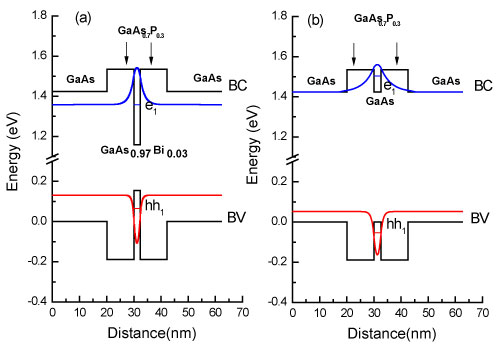
Quantum Well Design Studies
Our conceived laser structure is based upon of GaAsP/GaAsBi/GaAsP strain-compensated type-I active region. The central GaAs0.97Bi0.03QW whom the thickness is 2.5 nm is laminated between two 10 nm thick GaAs0.7P0.3 QWs which are in turn sandwiched by two 20 nm thick GaAs barriers that are lattice matched to the GaAs substrate. This structure is analyzed by comparing results to those obtained on Bi-free GaAsP/GaAs/GaAsP emitting at the same wavelength 0.796 µm at RT. The Figure 1 illustrates the schematic band diagram within the fundamental symmetric electron e1 and hole hh1 energy levels and their respective wave functions for the two laser structures, (a) Dilute-Bi and (b) Bi-free. The energy levels of these subbands have been calculated by solving the one-dimensional Schrödinger equation assuming the envelope function approximation [27,28]. The physical parameters used in the calculations are listed in Table 1. The conduction and valence band discontinuities ΔEC and ΔEV at hetero-interfaces, which are key parameters for the energy band diagram construction, were calculated by the density functional theory (DFT) and their values are listed in Table 2 [29,30]. Also, the band gaps of GaAs1-yPy and GaAs1-xBix strained to GaAs (001) were calculated using the following relationships, according to the DFT calculations and experimental fits are quoted from references [31, 32].
The dilute-bismide compound induces deep GaAsP/GaAsBi/GaAsP QW with high band offset value leading to good confinement of both types of carriers. The conduction and valence band-offse between GaAs and GaAsBi have been calculated and are, respectively, ΔEC = -265 meV and ΔEC = 155 meV. besides, in both the dilute-Bi or Bi-free laser structure, the active region is composed of type-I GaAsP/GaAsBi/GaAsP QWs. Subsequently, in this non-aligned configuration, the effective band gap seems to be independent of temperature and the laser emission wavelength could be easily tuned by tweaking the layer thickness of the GaAsP/GaAsBi/GaAsP period. These theoretical results indicate that a correctly selected GaAs1-yPy barrier provide band offsets much better than the thermal energy of RT even for the GaAs1-zBiz system with minor Bi incorporation. Furthermore, it is important to note that the potential barrier introduced by GaAs1-yPy could prevent carrier leakage, which will in opportunity, be expected to lead to an enhanced carrier injection efficiency and a better threshold current density at elevated temperature similar to that reported by reference [33] for InGaAsN lasers.
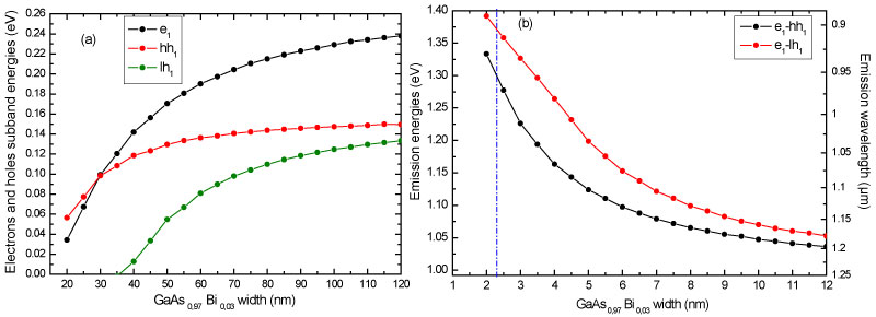
The energy levels of the different subband edges are represented in Figure 2. The latter plot shows that the quantum confinement energies of both types of carriers collapse with reduction of the GaAs0.97Bi0.03 layer width and attempt to stabilize from a thickness of 7 nm. Besides, it is shown on Figure 2a that for the GaAs0.97Bi0.03 layer thickness values less than the critical value of 7 nm, the energies vary in a nearly linear manner and rise with the GaAs0.97Bi0.03 layer width. In order to justify this behavior, we stipulate that the wave function of this state is localized in the GaAs0.97Bi0.03 layer mostly. It can also be seen on Figure 2b, that the emission energies decrease until GaAs0.97Bi0.03 layer thickness of 3.8 nm and then become constant and the interband transitions correspond then to the wavelength of 0.96 µm. Now that the GaAs0.97Bi0.03 layer is a deep quantum well for the holes, the wave function of the these carriers ground state is situated also in the GaAs0.97Bi0.03 layer. Thus, the transitions in such heterostructures are direct in the coordinate space (see Figure 1).
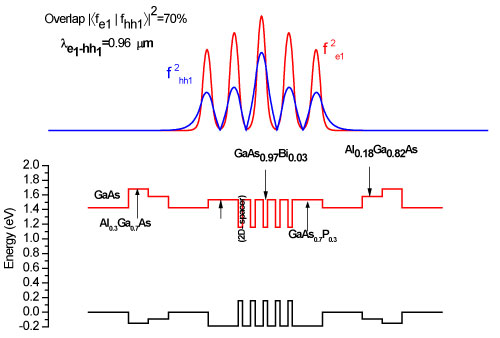
The present laser structure designed with bismide for infrared emission is made of GaAsP/GaAsBi/GaAsP type-I quantum wells. A 22 Å thick GaAsBi layer sandwiched by two 20 Å thick GaAs0.7P0.3layers. Each of GaAsP/GaAsBi/GaAsP quantum wells is separated by a 200 Å-thick GaAs spacer layer lattice-matched to the substrate. This feature confirms the bi-dimensional behavior of carriers in each MQW period. The dilute-bismide compound induces deep wells with high conduction and valence band offset values allowing strong confinement of both types of carriers. The GaAsP and GaAsBi layer thicknesses are chosen to exhibit laser emission around 0.96 µm at RT with the highest electron-hole wave-function overlap for the GaAsP/GaAsBi/GaAsP. This latter structure's active region is embedded in an undoped 100 Å-thick Al0.18Ga0.82. As waveguide layer whose the geometry enhances the optical confinement factor while minimizing free-carrier absorption losses in the Al0.3Ga0.7As cladding layer. This layer provides an improve of the optical confinement and high type-II band-offsets and let hope a reduction of the carriers leakage current. The Figure 3 shows the schematic band diagram of the dilute bismide laser structure with the fundamental electron e1 and heavy holes hh1 energy levels and their respective wave functions. The computation was performed using the Schrödinger equation and assuming the envelope function approximation [27].
Optical Gain and Radiative Current Calculation
The optical characteristics of the dilute-Bi GaAsP/GaAsBi/GaAsP structure are optimized in terms of modal gain and the threshold current density which is returned from optical gain calculation in TE mode polarization emission. For a quantum well, when kρ = 0, the optical gain energy spectra can have the following expression [34].
Where Δ(x) represents the Heaviside step function, fci and fvi are Fermi functions for the jth subband in the valence band and ith subband in the conduction band, respectively, |Iij|2 is the electron-hole wave function overlap|‹ψei|ψhi›|2, Eeihj is the energy corresponding to the optical transition starting from the conduction to the valence bands and :
Where is the electron-hole reduced effective mass, c, ω and ε are respectively the speed of light, the pulsation of light and the effective dielectric constant of the material; nAZ, Leff are the refractive index and the effective width of the active zone, respectively, and where Ep = (2/m0)P2 with P is the Kane matrix element.
In concerned cases, the optical gain has to be convoluted by some broadening function, so as to account for the limited lifetime of excitons. Thus, we shall use a Lorentzian shape for this broadening, with a half width at half maximum denoted by Γ. Also, we assume a Γ value equal to 26 meV leading to an intraband relaxation time τint which is worth 100 fs [34].
The optical gain is written as follow:
where is given by equation (3).
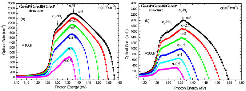
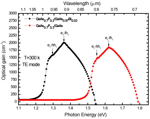
The optical gain per GaAs0.7P0.3/GaAs0.7P0.3/ GaAs0.97Bi0.03/GaAs0.7P0.3 period was calculated for different carrier injection densities σ in the active region varying from 0.5 × 10¹² to 3 × 1012 cm-2 Obtained results are plotted in Figure 4 at low (T = 100 K) and RT (T = 300 K). At low temperature on Figure 4a, we guess that, it is easy to get gain because the difference between electron and hole quasi-Fermi energies (Efc - Efv) reaches the (e1-lh1) transition energy starting from the carrier injection of σ = 0.5 × 1012 cm-2. On the other hand, at RT Figure 4b, it is compulsory to have an injection rate of at least σ = 1 × 1012 cm-2 to allow to carriers to fulfill stimulated emission conditions. Whatever the temperature, the maximum gain Gmax due to the first energy level corresponding to the transition (e1-hh1) increases quasi-linearly with the injected carrier density. This gain peak is dominated at low temperature by the (e1-lh1) transition only for lower injection rates. Furthermore, At σ = 1.5 × 1012 cm-2, the gain from the second quantized level transition (e1-lh1) involving light hole carriers becomes significant. Moreover, The transparency carrier density is equal to 0.25 × 1012 cm-2 at RT. For a typical injected carrier density of 2 × 1012 cm-2, a gain value of about 1500 cm-1 is obtained, which is sensibly comparable to values obtained on GaSbBi/GaSb structure tailored for emission at 2 μm (E = 0.62 eV) on GaSb substrate [35]. This steep gain value could be attributed to the 2D density of states which is proportional to the effective masses and inversely proportional to the confinement energy of electron and hole as well as to the quasi-Fermi levels [36]. From the viewpoint of applications, the optical quality of dilute bismide in lasers is a very valuable issue. Indeed, for GaAsBi and InPBi, this quality dwindles very significantly due to incorporation of Bi atoms [37]. The Figure 5 shows the optical gain spectra of the two laser structures, with dilute-Bi and Bi-free. For two-dimensional system, carrier densities N2D is rises up to 3 × 1012 cm-2. In the case of the dilute-Bi structure, the conduction subbands e1 and e2 are clearly splitted, consequently; for the used carrier densities in our calculations, only e1 and hh1 levels are occupied. Thus, the peak in the gain curve corresponds to (e1-hh1) transition. Also, we note an improvement of optical gain values and a red shift of the gain spectrum to higher wavelengths in the based GaAsBi QW laser structure [38]. The latter could be explained by the large bowing factor of the GaAsBi energy band gap. For dilute-Bi structure, a gain value at around of 2000 cm-1 is attained with a typical injected carrier density of 3 × 1012 cm-2. This result is comparable to those obtained on the GaSbBi/GaSb structure adapted for emission at 2 μm on GaSb substrate but higher than those obtained for Bi-free structure as illustrated in Figure 5. These previous high gain values could be attributed in part to the electron mass enhancement as well as the increase in density of states in dilute-bismide compounds. For the Bi-free structure, when the carrier density is 3 × 1012 cm-2, the gain peak corresponding to (e1-lh1) transition occurs at about 1.4259 eV and is larger than that of dilute-Bi which is worth 1.38 eV for the same carrier density. Moreover, for the Bi-free structure, the transition between the occupied e1 and the unoccupied e2 is unlikely. Thus, the difference in shape between the corresponding black and red curves could be interpreted by band filling and the resulting shift of the quasi-Fermi energy separation. Due to the variation of the effective mass at the level of the valence band in GaAsBi with the incorporation of bismide as well as the densities of states, these results leading to a higher transparency current similar to InGaAs-based laser structures [39,40].
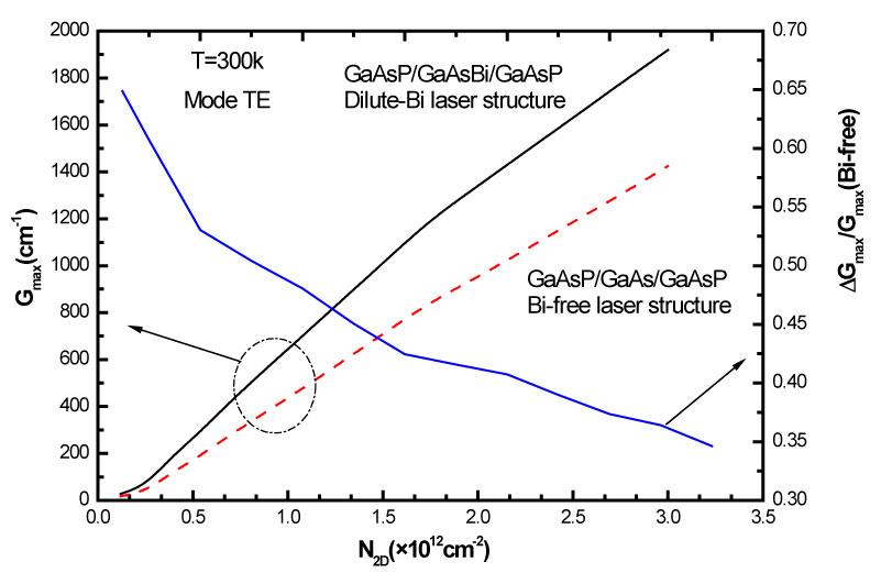
In addition the optical gain of GaAsBi-based laser structure is comparable with the optical gain values in InGaAs-based devices [36]. Calculated maximum gain as a function of carrier density is illustrated in Figure 6 for both structures at RT. This shows the superiority of the dilute-Bi structure in comparison to the Bi-free one, whatever these have the same carrier density. In the case of a carrier density equal to 3 × 1012 cm-2, the incorporation of bismide in GaAs well (GaAsBi) induces an enhancement in the Gmax value. The transparency carrier density is 5.5 × 1018 cm-3 for the dilute Bi and 5.42 × 1018 cm-3 for the Bi-free structures. These latter values are obtained using the relation N3D=N2D/Leff, where Leff is the effective width of the structure equal to 222 Å and 225 Å for dilute-Bi and Bi-free structures, respectively.
It is well acknowledged that the suitable part of the optical gain (modal gain) has to recompense the total optical losses (α), of the laser diode for this reason we,
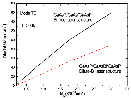
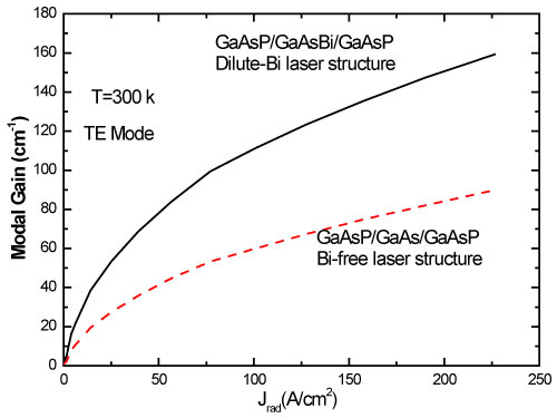
The most interesting result was obtained for dilute-Bi structure with a Γp value per period of 1.66% while Γp is equal to1.26% for the Bi-free structure [41]. The Figure 7 illustrates the variation of modal gain versus carrier concentration N3D for dilute-Bi and Bi-free structures. Unsurprisingly, the maximum modal gain value is accomplished GaAsP/GaAsBi/GaAsP laser design. For a typical carrier concentration N3D = 1 × 10¹⁸ m-3 (σ = 1 × 10¹² m-3), the modal gain at T = 300K exceeds 54 cm-1, whereas it reaches only 28 cm-1 for the Bi-free structure. Thus, this result confirms the valued effect of the dilute-bismide incorporation in the active region of laser structure and corroborates the possibility to obtain, at RT, a laser structure operating with reasonable optical losses. Starting from the relation Gmad = GpNpGmax, we have performed the calculation the modal gain Gmad where Gmax is the peak gain value found out from the optical gain curves (Figure 5), Np is the quantum wells number taken equal to 5 and Gp is the TE polarization optical confinement factor. Moreover, it was computed using the refractive indices nop extracted from Table 1, following the procedure assumed in Ref. [24]. The carried out calculations at 300K indicated that the incorporation of bismide reduces the radiative efficiency of the structure (Figure 8a). By assuming uniform charge injection across the laser active region, we can use the simplified expression of spontaneous emission rate given by [42].
Where c is the speed of light, nr are the refractive index, m0 is the free-electron mass, is the squared momentum matrix element between electron and hole in each sub-band averaged over directions and polarizations of photons and spins of electrons and holes, ρred is the reduced density of state of electrons and holes in the xy plan without spin degeneracy, Fc,v is the quasi-Fermi level of conduction and valence band and f(E) the Fermi-Dirac distribution function ρred is written as mred/2πℏ2 through the effective mass approximation, where mred is reduced mass of electrons and holes in the xy plane. is estimated by the k•p theory to be :
Where mc is the electron effective mass, Eg the band gap energy, Δ the spin-orbit splitting and ηc-v the overlap integral of the envelope function of the electrons and holes, respectively. A low bound on the threshold current density may be obtained by calculating the radiative recombination rate per unit volume given by [42].
Where E is the photon energy. The performed calculation results at 300 K leads to believe that the addition of bismide degrades the radiative efficiency of the structures (Figure 8a). By taking into account uniform charge injection across the laser active region, we can use the simplified expression:
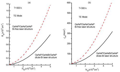
The radiative recombination coefficient B at RT equal to 3.6 × 10⁻¹¹ and 7.076 × 10⁻¹¹ cm3s-1, respectively, for dilute-Bi and Bi-free laser structures, in agreement with standard values of GaAs laser structures [43,44]. Furthermore, the radiative current density Jrad could be calculated by integrating over the spontaneous emission spectrum at each value of N3D [45], it comes:
where e is the electron charge and Lz = NpLeff is the total active region. For typical injected carrier density N3D = 2.5 × 1018 cm-3, typical for laser diode operation at RT. The Jrad values are always less than 100 A/cm2 for the dilute-Bi structure, confirming the possibility to such laser diode to operate at RT. These relevant results are illustrated in Figure 8b, where the modal gain Gmod versus the radiative current density Jrad at 300 K for the two LDs under consideration at RT indicate in Figure 9. The result reported in Figure 9 demonstrates that modal gain is better for the dilute-Bi structure, about two times higher than the Bi-free structure all over the Jrad values. Keeping in view reasonable total optical losses at around 10-15 cm-1 for a low-defect laser structure operating at RT [46], the Jrad value is deduced for the dilute-Bi structure two times lower than the Bi-free one. Basing upon these theoretical investigations, it can be guessed that GaAsBi/GaAs quantum well lasers structures are a promising new class of near-infrared devices where, by use of the unusual band structure properties of GaAsBi alloys, it is possible to eliminate the dominant energy-consuming Auger recombination and inter-valence band absorption loss mechanisms, which have a great impact on the device performance [47]. We emphasize that the inhibition of these loss mechanisms let us hope GaAsBi to be the potential candidate for the development of next-generation semiconductor lasers. The precise estimation of the Auger coefficient in the diluted-Bi laser structures will be the subject of future studies.
Conclusion
A new dilute-Bi type-I GaAs0.7P0.3/GaAs0.97Bi0.03 laser structure has been proposed and optimized for emission at 0.960 μm and at RT in order to show an appropriate overlap wave functions value equal to 70%. The theoretical performances of such laser structure are compared to a similar conventional Bi-free structure for laser operation at RT. The results obtained on the calculation of the optical gain for the two laser structures show the superiority of the bismuth system due to the increased effective mass of the edge of the valance band in the GaAsBi layer and the improved optical density of states in dilute-Bi compounds. As a consequence, the dilute-Bi laser structure presents high optical material gain around 1000 cm-1, modal gain value is equal to 80 cm-1 and radiative current density below 100 A/cm2 at 300 K for typical injected carrier concentration N3D = 1.5 × 1013 cm-3. These results approve that the GaAsP/GaAsBi structure are of an excessive attention for the realization of laser devices operating in the near-infrared region at RT.
References
- Takamoto T, Kaneiwa M, Imaizumi M, et al. (2005) InGaP/GaAs-based multijunction solar cells. Prog Photovoltaics 13: 495.
- Yamaguchi M, Nishimura K, Sasaki T, et al. (2008) Investigation of LPE grown dilute nitride InGaAs(Sb)N layers for photovoltaic applications. Sol Energy 82: 173.
- Dimroth F (2006) High‐efficiency solar cells from III‐V compound semiconductors. Phys Status Solidi C 3: 373.
- Bertulis K, Krotkus A, Aleksejenko G, et al. (2006) GaBiAs: A material for optoelectronic terahertz devices Appl Phys Lett 88: 201112.
- Tominaga Y, Kinoshita Y, Oe K, et al. (2008) Structural investigation of GaAs1−xBix/GaAs multiquantum wells. Appl Phys Lett 93: 131915.
- Fluegel B, Francoeur S, Mascarenhas A, et al. (2006) Giant spin-orbit bowing in GaAs1−xBix. Phys Rev Lett 97: 067205.
- Lu XF, Beaton DA, Lewis RB, et al. (2009) Composition dependence of photoluminescence of GaAs1−xBix alloys. Appl Phys Lett 95: 041903.
- Mohmad AR, Bastiman F, Ng JS, et al. (2011) The effect of Bi composition to the optical quality of GaAs1−xBix. Appl Phys Lett 98: 122107.
- Yeh JY, Mawst LJ, Khandekar AA, et al. (2006) Characteristics of InGaAsN-GaAsSb type-II "W" quantum wells. J Cryst Growth 287: 615-619.
- Chen B (2017) Optical gain analysis of GaAs-based InGaAs/GaAsSbBi type-II quantum wells lasers Optics Express 25: 25183-25192.
- Alberi K, Wu J, Walukiewicz W, et al. (2007) Valence-band anticrossing in mismatched III-V semiconductor alloys. Phys Rev B 75: 045203.
- Lewis R, Beaton D, Lu X, et al. (2009) GaAs1−xBix light emitting diodes. J Cryst Growth 311: 1872.
- Hossain N, Marko IP, Jin SR, et al. (2012) Recombination mechanisms and band alignment of GaAs1−xBix/GaAs light emitting diodes. Appl Phys Lett 100: 51105.
- Tominaga Y, Oe K, Yoshimoto M (2010) Low temperature dependence of oscillation wavelength in GaAs1-xBix laser by photo-pumping. Appl Phys Express 3: 62201.
- Ludewig P, Knaub N, Hossain N, et al. (2013) Electrical injection Ga(AsBi)/(AlGa)As single quantum well laser. Appl Phys Lett 102: 242115.
- Lu X, Beaton DA, Lewis RB, et al. (2008) Effect of molecular beam epitaxy growth conditions on the Bi content of GaAs1−xBix Appl Phys Lett 92: 192110.
- Pacebutas V, Bertulis K, Aleksejenko G, et al. (2009) Molecular-beam-epitaxy grown GaBiAs for terahertz optoelectronic applications. J Mater Sci Mater Electron 20: 363-366.
- Imhof S, Thranhardt A, Chernikov A, et al. (2010) Clustering effects in Ga(AsBi). Appl Phys Lett 96: 131115.
- Grein CH, John S (1989) Temperature dependence of the Urbach optical absorption edge: A theory of multiple phonon absorption and emission sidebands. Phys Rev B 39: 1140.
- Hjalmarson H, Vogl P, Wolford DJ, et al. (1980) Theory of substitutional deep traps in covalent semiconductors. Phys Rev Lett 44: 810.
- Shen J, Ren SY, Dow JD (1990) Relaxed-lattice model of isolated and paired isoelectronic traps in GaP. Phys Rev B Condens Matter 42: 9119-9126.
- Francoeur S, Tixier S, Young E, et al. (2008) Bi isoelectronic impurities in GaAs. Phys Rev B 77: 085209.
- Forghani K, Guan Y, Losurdo M, et al. (2014) GaAs1−y−zPyBiz, an alternative reduced band gap alloy system lattice-matched to GaAs. Appl Phys Lett 105: 111101.
- Harbi N, Sfina N, Jbeli A, et al. (2015) Direct band gap Inx Ga1−x As/Ge type II strained quantum wells for short-wave infrared p–i–n photodetector. Optical Materials 46: 472-480.
- Joullie A, Christol P (2003) GaSb-based mid-infrared 2–5 μm laser diodesDiodes laser à base GaSb pour moyen infrarouge (2–5 μm). C R Phys 4: 621-637.
- Ferhat M, Zaoui A (2006) Structural and electronic properties of III-V bismuth compounds. Phys Rev B 73: 115107.
- Alberi K, Walukiewicz W, Yu KM, et al. (2007) Haas measurement of electron effective mass in GaAs1−xBix. Appl Phys Lett 91: 051909.
- Usman M, Broderick CA, Batool Z, et al. (2013) Impact of alloy disorder on the band structure of compressively strained GaBixAs1−x. Phys Rev B 87: 115104.
- Kopaczek J, Kudrawiec R, Polak MP, et al. (2014) Contactless electroreflectance and theoretical studies of band gap and spin-orbit splitting in InP1−xBix dilute bismide with x ≤ 0.034. Appl Phys Lett 105: 222104.
- Kim H, ForghaniK, Guan Y, et al. (2015) Strain-compensated GaAs1−yPy/GaAs1−zBiz/GaAs1−yPy quantum wells for laser applications. Semicond Sci Technol 30: 094011.
- Ahn D, Chuang SL (1990) Optical gain and gain suppression of quantum-well lasers with valence band mixing. IEEE J Quantum Electron 26: 13-24.
- Tansu N, Mawst LJ (2005) Current injection efficiency of InGaAsN quantum-well lasers. J Appl Phy 97: 054502.
- Robert C, Perrin M, Cornet C, et al. (2012) Atomistic calculations of Ga(NAsP)/GaP(N) quantum wells on silicon substrate: Band structure and optical gain. Appl Phys Lett 100: 111901.
- Gladysiewicz M, Kudrawiec R, Miloszewski JM, et al. (2013) Band structure and the optical gain of GaInNAs/GaAs quantum wells modeled within 10-band and 8-band kp model. J Appl Phys 113: 063514.
- A Ben Ahmed, H Saidi, et al. (2015) Band structure, optical transition, and optical gain of Type-II InAs(N)/GaSb quantum wells laser diodes modeled within 16-band and 14-band kp model. IEEE J Quantum Electron 51: 2500108.
- Igor P Marko, Christopher A Broderick, Shirong Jin, et al. (2016) Optical gain in GaAsBi/GaAs quantum well diode lasers Sci Rep 6: 28863.
- Tourniee E, Baranov AN (2012) Chapter 5 - Mid-infrared semiconductor lasers: A review. Semiconductors and Semimetals 86: 183-226.
- Igor P Marko, Stephen J Sweeney (2017) Progress Toward III–V Bismide Alloys for Near- and Midinfrared Laser Diodes. IEEE J Sel Top Quant Electron 23: 1501512.
- Tsvid G, Kirch J, Mawst LJ, et al. ( 2008) Spontaneous radiative efficiency and gain characteristics of strained-layer InGaAs–GaAs quantum-well lasers. IEEE J Quantum Electron 44: 732.
- Chuang SL (1995) Physics of optoelectronic devices, Wiley Series in Pure and Applied Optics, New York.
- Lash G, Stern F (1964) Spontaneous and stimulated recombination radiation in semiconductors. Phys Rev A 133: 553-563.
- Bebb HR, Wiliams EW (1972) Semiconductors and Semimetals. In: Willardson RK Beer AC, Academic, New York.
- Christol C, Bigenwald P, Joullie A, et al. (1999) Improvement of Sb-based multiquantum well lasers by Coulomb enhancement. IEE Proc Optoelectron 146: 3-8.
- Christopher A Broderick, Patrick E Harnedy, Eoin PO'Reilly (2015) Theory of the Electronic and Optical Properties of Dilute Bismide Quantum Well Lasers. IEEE Quntum electronics 21.
- Bishop PJ, Daniels ME, Ridley BK, et al. (1992) Radiative recombination in GaAs/AlxGa1−xAs quantum wells. Phys Rev B 45: 6686.
- Fluegel B, Francoeur S, Mascarenhas A, et al. (2006) Giant Spin-Orbit Bowing in GaAs1−xBix. Phys Rev Lett 97: 067205.
- Imhof S, Buckers C, Thranhardt A, et al. (2008) Microscopic theory of the optical properties of Ga(AsBi)/GaAs quantum wells. Semicond Sci Technol 23: 125009.
Corresponding Author
Noureddine Sfina, Laboratoire de la Matière Condensée et des Nanosciences (LMCN), Département de Physique, Faculté des Sciences de Monastir, Université de Monastir, Avenue de l'Environnement, 5019 Monastir, Tunisia; Faculty of science and art KKU Mahail Assir, King Khalid University, Saudi Arabia.
Copyright
© 2019 Sfina N. This is an open-access article distributed under the terms of the Creative Commons Attribution License, which permits unrestricted use, distribution, and reproduction in any medium, provided the original author and source are credited.